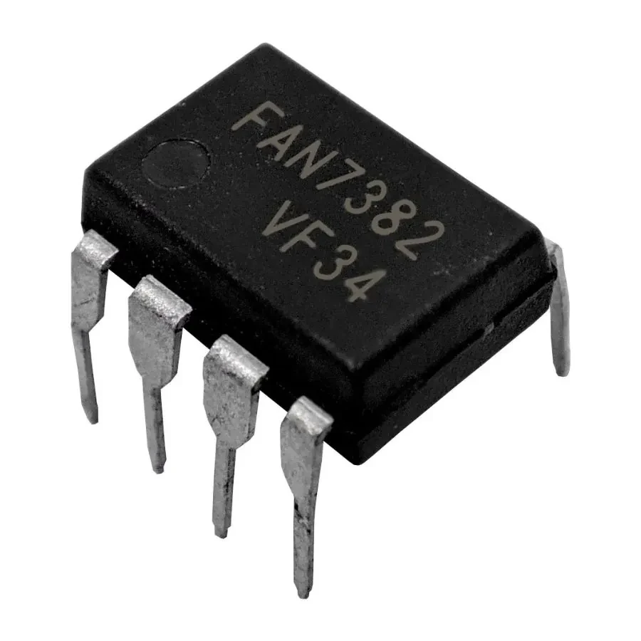
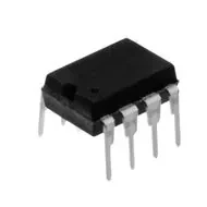
FAN7382 Half-Bridge Gate-Driver IC
Inhouse product
Reviews & Ratings
the FAN7382, a popular half-bridge gate driver IC from onsemi (formerly Fairchild Semiconductor).
Overview
The FAN7382 is a monolithic high-voltage gate drive IC designed to drive both high-side and low-side N-Channel MOSFETs or IGBTs in a half-bridge configuration. It is widely used in switching power applications such as motor drives, power supplies, and inverters for appliances and industrial systems.
Its key function is to translate low-power logic signals from a microcontroller (MCU) or PWM controller into high-current, high-voltage signals necessary to rapidly switch power transistors on and off.
Key Features:
High-Voltage Operation: Features a high-side floating channel designed for bootstrap operation, allowing it to drive a high-side switch with a voltage up to +600V.
Wide Supply Voltage Range (VCC): The logic and low-side driver operates from 10V to 20V, making it compatible with standard 12V or 15V gate drive supplies.
High Output Current: Capable of sourcing/sinking +250 mA / -350 mA peak current. This allows for fast switching of large MOSFET/IGBT gates, minimizing switching losses.
Matched Propagation Delays: The propagation delays for the high-side and low-side channels are closely matched (< 50 ns), which is critical for preventing shoot-through currents in the half-bridge.
Integrated Dead Time: An internal dead time (typically 540 ns) is generated between the shut-down of one transistor and the turn-on of its complementary partner. This is a crucial safety feature to prevent both transistors in the same leg from being on simultaneously (shoot-through), which would cause a catastrophic short circuit.
Under-Voltage Lockout (UVLO): For both the high-side and low-side drivers. If the supply voltage (VCC) drops below a specified threshold (typically ~8.7V), the outputs are disabled, preventing the power switches from operating in a linear (high-loss) region, which could destroy them.
dv/dt Immunity: The high-side channel is immune to high voltage transient conditions, ensuring stable operation under noisy switching conditions.
CMOS/LSTTL Compatible Inputs: The input pins are compatible with standard 3.3V and 5V logic levels, allowing for direct interfacing with microcontrollers and DSPs.
Pin Configuration (Typically an 8-pin DIP or SOIC)
| Pin # | Pin Name | Function |
|---|---|---|
| 1 | VCC | Low-side and control logic supply voltage (typically +12V to +15V). |
| 2 | HIN | High-side Input: Logic input to control the high-side output (HO). |
| 3 | LIN | Low-side Input: Logic input to control the low-side output (LO). |
| 4 | GND | Ground reference for the IC's control logic and low-side driver. |
| 5 | LO | Low-side Output: Connects directly to the gate of the low-side MOSFET/IGBT. |
| 6 | VS | High-side Floating Supply Return: The return path for the high-side driver; connected to the switch node (the source of the high-side MOSFET). |
| 7 | HO | High-side Output: Connects directly to the gate of the high-side MOSFET/IGBT. |
| 8 | VB | High-side Floating Supply: The positive supply voltage for the high-side driver; connected to the bootstrap capacitor. |
Internal Block Diagram and How It Works
A simplified explanation of its operation:
Input Stage: The logic signals at HIN and LIN are received. The internal logic processes these signals, ensuring they are level-shifted to the correct voltages for the high- and low-side drivers.
Dead Time Generation: The internal circuitry automatically inserts a fixed dead time between the falling edge of one signal and the rising edge of the complementary signal.
Output Drivers:
The Low-Side Driver is referenced to GND. It directly drives the LO pin.
The High-Side Driver is a "floating" circuit referenced to the VS pin (the switch node). Its power comes from the voltage between VB and VS. This is generated using a bootstrap circuit.
Bootstrap Circuitry (External): This is a critical part of using the FAN7382. It consists of a bootstrap diode (D_BS) and a bootstrap capacitor (C_BS).
When the low-side switch (Q2) is ON, the VS pin is pulled close to GND.
This allows the VCC supply to charge the capacitor (C_BS) through the diode (D_BS), building up a voltage of ~VCC across it.
When the high-side needs to be turned on, the driver uses the charge stored in C_BS to power the high-side gate drive circuit. The voltage at VB becomes
VS + V_CBS, providing the necessary voltage to drive the high-side gate above the switch node voltage (VS).
Frequently Bought Products
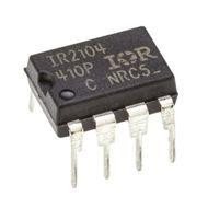
IR2104 Half Bridge Driver IC
Product Queries (0)
Login Or Registerto submit your questions to seller
Other Questions
No none asked to seller yet